VLSI & digital design Student VLSI study
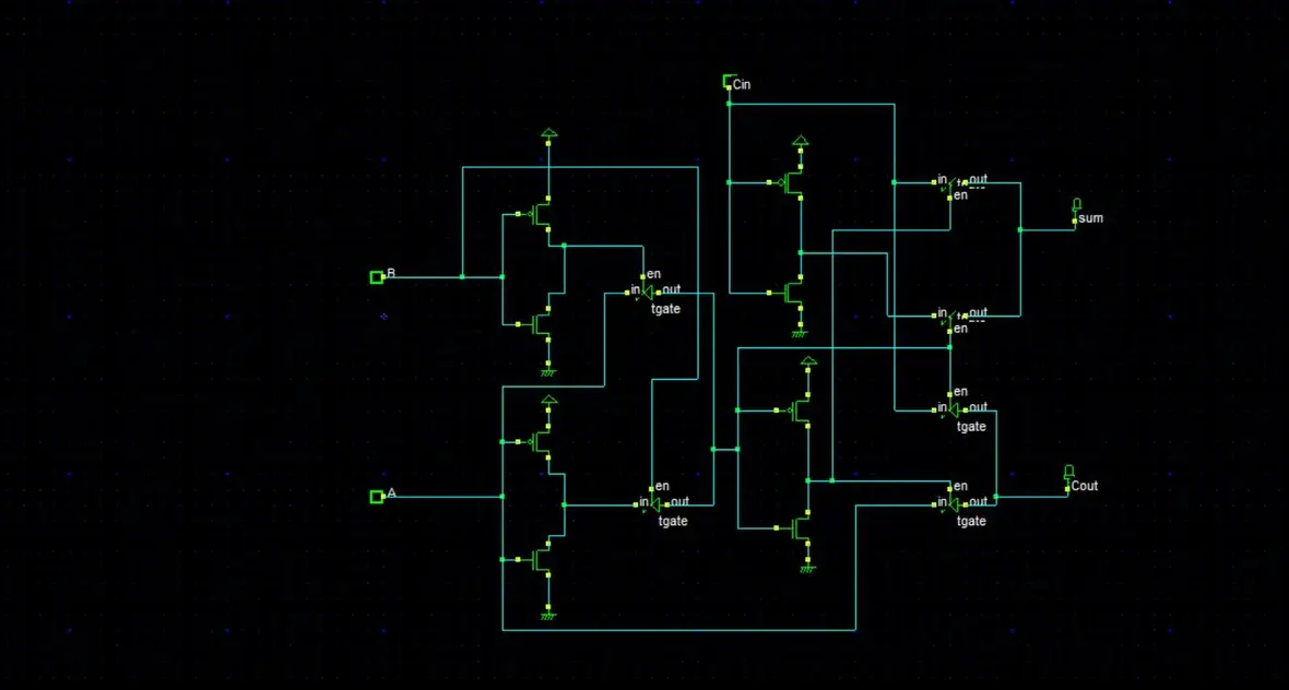
Low-Power CMOS Full Adder
A circuit study comparing transmission gate logic with a conventional CMOS full adder.

The brief
Explore a lower-power implementation of the arithmetic circuit that adds one bit and a carry input.
How it works
- Design a full adder using transmission gates
- Compare against a conventional CMOS implementation
- Review logic outputs and physical layout in simulation
Want to build something similar?
Send your own project title and target budget.